


AFS Solutions Complete Laptop Course 8 hours
On Sale
$15.00
$15.00
Preview
- » Understanding of schematics Diagram on the live practical Motherboard and its important Voltage and signals.
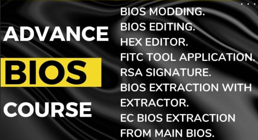
- » BIOS ME region Cleaning including CSME & TXE region (6th, 7th, 8th, 9th gen).
- » ALL CHARGING IC's ( Bq24725/Bq24707A ,Bq24735 Bq24745, Bq24751etc) working, Internal logic, Schematics and Troubleshooting of various Charging problem.
- » ALL 3.3/5 V Buck regulator IC's (TPS51225 TPS51223, RT8205A/B/C, RT8206A/B, NB670 etc.) working , internal logic, schematics and Troubleshooting .
- » Power-On sequence of ALL generations With SOC(system on chip) Structure Motherboard. With different states (S0, S3, S4, S5, G2, G3).
- » Feedback voltage, MODE, TRIP, I2C, SMBus, LPC, PCI Signal functions Logic.
- » Various sections including S/B section, Charging section, RTC section, VGA CORE section, RAM section, LVDS section etc Signal, Voltage CLOCK and DATA description .
- » All signals working in schematics e.g - PLTRST#, RSMRST#, VCCRTC, SRTRST#, RTC SUSCLK, X1 & X2, INTRUDER#, INTVRMEN, SYS_ON, RUN_ON, DDR_PWR_OK, VGA_OK, S_PGOOD, RAMRST, SUSP#, 51ON etc.
- » Switching of OP-Amp (Comparator), Diode, MOSFET( E-MOS, D-MOS, C-MOS), Transistor (BJT), in schematics.
- » Graphic to non-graphic conversion and ASUS onboard RAM disable method.
- » Learn the concept and be an EXPERT don't opt for HIT and TRIAL.